SPI modes
Let’s break down SPI modes slowly and cleanly from physical signals, timing, interpretation, real MCU usage.
Let’s break down SPI modes slowly and cleanly — from physical signals → timing → interpretation → real MCU usage.
What SPI “Mode” Actually Means
SPI has two timing parameters that define when data is sampled and what level the clock idles at.
Those two parameters are:
- CPOL → Clock Polarity
- CPHA → Clock Phase
Together, they define the SPI Mode.
CPOL — Clock Polarity
- Decides the idle state of the clock (SCLK).
- It doesn’t affect data, only the base level of the clock when nothing’s happening.
| CPOL | Clock idle state | Active edge direction |
|---|---|---|
| 0 | Idle Low (starts from 0) | Active edge = rising edge |
| 1 | Idle High (starts from 1) | Active edge = falling edge |
CPHA — Clock Phase
- Decides when the data is sampled (read) and when it is shifted (written).
- In simple words: “Should I read data on the first clock edge or the second clock edge?”
| CPHA | Sampling edge | Shifting edge |
|---|---|---|
| 0 | 1st edge | 2nd edge |
| 1 | 2nd edge | 1st edge |
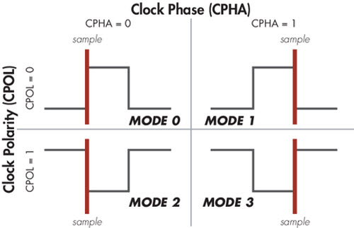
Combine CPOL and CPHA → 4 SPI Modes
| Mode | CPOL | CPHA | Clock Idle | Data Sample Edge | Description |
|---|---|---|---|---|---|
| 0 | 0 | 0 | Low | Rising edge | Data valid on rising edge, change on falling edge |
| 1 | 0 | 1 | Low | Falling edge | Data valid on falling edge, change on rising edge |
| 2 | 1 | 0 | High | Falling edge | Data valid on falling edge, change on rising edge |
| 3 | 1 | 1 | High | Rising edge | Data valid on rising edge, change on falling edge |
Visualization (conceptual)
Let’s imagine one bit transfer (Master → Slave):
Mode 0 (CPOL=0, CPHA=0)
1
2
3
Clock:  _-_-_-_-_
Data :  D7       D6       D5 ...
Sample ↑
Mode 3 (CPOL=1, CPHA=1)
1
2
3
Clock:  -_-_-_-_-
Data :      D7       D6 ...
Sample ↑
- When CPOL=0, clock idles low → active high pulses.
- When CPOL=1, clock idles high → active low pulses.
- CPHA decides whether the first edge is “sample” or “setup”.
Practical Tip
Different SPI slaves require different modes — for example:
| Device | Typical SPI Mode |
|---|---|
| Flash memory (W25Qxx) | Mode 0 or 3 |
| Accelerometer (ADXL345) | Mode 3 |
| MCP3008 ADC | Mode 0 |
| DAC MCP4921 | Mode 0 |
Always check the slave datasheet timing diagram to match CPOL/CPHA.
If you mismatch it:
- Data gets shifted by half a clock — causing garbage reads.
- Typical symptom: every byte is wrong, but consistently wrong.
Example on RA6E1 (or STM32-style pseudocode)
1
2
3
4
5
6
7
8
9
spi_cfg_t cfg = {
    .channel        = 0,
    .clk_phase      = SPI_CLK_PHASE_EDGE_ODD,   // CPHA = 1
    .clk_polarity   = SPI_CLK_POLARITY_HIGH,     // CPOL = 1
    .bit_order      = SPI_BIT_ORDER_MSB_FIRST,
    .bitrate        = 1000000,                   // 1 MHz
    .operating_mode = SPI_MODE_MASTER
};
R_SPI_Open(&g_spi_ctrl, &cfg);
Rule of Thumb to Remember
| Mode | Clock idle | Sample edge | When to use |
|---|---|---|---|
| 0 | Low | Rising | Default safe mode |
| 1 | Low | Falling | If data valid after 1st edge |
| 2 | High | Falling | Rare; check datasheet |
| 3 | High | Rising | Flash memories, sensors |
Interview Insight
If interviewer asks:
“What happens if CPOL or CPHA mismatch between master and slave?”
You say:
“The master and slave will interpret data bits at different clock edges, causing bit misalignment — effectively corrupting every byte. You’ll see shifted data or fixed wrong values.”